Supplier sections
Rate this page
Analog Devices simplifies high-speed data converter-to-FPGA interconnect design environment

Communications infrastructure, imaging equipment, industrial instrumentation, defence electronics and other multi-channel, data-hungry systems are demanding wider resolutions and higher sampling rates from the data conversion stage. Physical layout constraints of the parallel interface and bit-rate limitations of the serial LVDS (low-voltage differential signaling) approach are beginning to present technical barriers for designers.
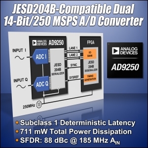
To address this need, Analog Devices has introduced the AD9250 dual-channel, 14-bit, 250-MSP A/D converter featuring the JEDEC JESD204B serial output data interface standard. The AD9250 A/D converter is the first-to-market with full JESD204B Subclass 1 deterministic latency at 250 MSPS. This functionality accommodates the precise synchronisation of multiple data-conversion channels through a serial interface.
- Download AD9250 data sheet
- Learn more about ADI’s JESD204 serial interface technology
- Watch the webcast "Demystifying the JESD204B High-speed Data Converter-to-FPGA Interface"
The AD9250 A/D converter’s serial interface implementation provides up to 5 Gbps over a 1 or 2 lane-capable link. Two serial lanes are used to support the full 250-MSPS, dual A/D converter data rate, or a single lane can be used to support reduced sampling rates.
High-performance FPGA suppliers, such as Xilinx Inc., have incorporated on-chip JESD204B SerDes (serialiser/deserialiser) ports into their latest generation products. This end-to-end seamless connectivity for the analog signal chain results in simplified PCB layout, rapid prototyping capability and faster time-to-market.
“Xilinx is fully-committed to supporting the JEDEC JESD204B standard and is striving to accelerate adoption of the serialised interconnect technology for data converters. We are doing this by providing high quality, flexible, scalable and programmable IP to interface with high speed data converters like the AD9250,” said Sunil Kar, senior director, Wireless Business Group at Xilinx. “Xilinx currently provides JEDEC JESD204B IP for Subclass 0, 1 and 2 functionality, with line rates up to 10.3 GBPS and lane widths ranging from x1 to x8 on our devices. This combination of technology advancements improves system modularisation, lowers cost and complexity and will enhance the capabilities and capacities of next generation wireless and wired networks.”
“This flagship product from Analog Devices signals a new, tightly integrated approach to designing the analog signal chain in FPGA-based systems,” said Kevin Kattmann, product line director, High-speed A/D Converters at Analog Devices. “The AD9250 dual 14-bit A/D converter delivers unmatched wideband signal processing performance while its simplified interface breaks design barriers for next-generation FPGA-based applications in software-defined radio and medical ultrasound. For many system designers, the I/O challenge in implementing the high-performance analog signal chain now has an elegant solution.”
More About the AD9250 Dual-channel 14-bit, 250-MSPS A/D Converter
The AD9250 converter’s JESD204B serial interface reduces the number of high-speed differential output data paths required from as many as 28 to just two per IC. Its Subclass 1 deterministic latency function is repeatable from power-up cycle to power-up cycle and across link re-synchronisation events. Areas where this function is important are in diversity radio systems and instrumentation, multi-mode digital receiver applications such as TD-SCDMA, WCDMA, LTE (especially the 2R2T >8R8T evolution), radar/defence electronics, medical imaging systems, cable infrastructure and general-purpose software radios.
AD9250 Dual-channel 14-bit, 250-MSPS A/D Converter Key Features and Performance
- JESD204B coded serial digital output with Subclass 1 deterministic latency
- SNR = 70.6 dBFS at 185 MHz AIN and 250 MSPS
- SFDR = 88 dBc at 185 MHz AIN and 250 MSPS
- IF sampling frequencies of up to 400 MHz
- 95-dB channel isolation/crosstalk
- Low power and small package size
Evaluation Kits
The AD9250-250EBZ (250 MSPS), AD9250-170EBZ (170 MSPS), and AD6673-250EBZ DUT boards, and companion HSC-ADC-EVALDZ high-speed data capture card, comprise a signal performance-optimised complete evaluation system for the AD9250. The captured data can be analysed using a laptop computer and ADI’s free VisualAnalog™ software. For compatibility with FPGA development platforms, the CVT-ADC-FMC-INTPZB FMC interposer connector for the DUT boards is available.
Complementary Components
The AD9250 dual-channel 14-bit, 250-MSPS A/D converter works well with other Analog Devices components, including the AD8138, ADA4937, and ADA4938-2 drivers for baseband differential analog input configurations, and the AD9516-3 clock distribution IC with ADCLK905 low-jitter clock buffer.
A 170-MSPS pin-compatible version (AD9250-170) is available, as well as the AD6673, an 11-bit, 250-MSPS, pin-compatible version.
All devices are supplied in a 48-lead LFCSP package.
For more information, or details on the full range of Analog Devices products available from Anglia, please email info@anglia.com
This news article was originally published in April 2013.


