Supplier sections
Rate this page
Toshiba MOSFETs target power management application with smallest package

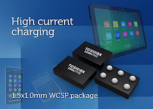
Toshiba has announced two ultra-compact MOSFETs in high power dissipation packages that have been specifically developed to meet the high-current charging requirements of the latest mobile devices.
The SSM6K781G N-channel and SSM6J771G P-channel MOSFETs are each supplied in a miniature 1.5mm x 1.0mm wafer level chip scale package (WCSP6C) package that is rated for power dissipation (PD) of up to 1.2W. The WCSP6C package is the optimum choice in applications with minimum available board space, as the ratio between size and power handling capability of the WCSP6C package is superior in comparison to mold type packages. This makes the MOSFETs ideal for power switching in charging circuits for the latest tablets, mobile phones and other space-constrained portable devices where high currents are required to minimise charge times.
Toshiba's new devices combine a low on resistance (RDS(ON)) with a very low capacitance and can be used in battery charging and DC/DC converter architectures. Typical RDS(ON) ratings are 14.4mOhm (VGSS = 4.5V) for the N-channel SSM6K781G and 26mOhm (VGSS = -4.5V) for the P-channel SSM6J771G.
The SSM6K781G MOSFET has a maximum DC current rating of 7A, while the SSM6J771G can handle up to -5A with the SSM6J771G being especially suitable for dual-cell charging applications due to its maximum gate source voltage rating of VGSS = +/-12V.
For more information, or details on the full range of Toshiba products available from Anglia, please email info@anglia.com
This news article was originally published in October 2014.


